Precision machining inspection systemのメーカーや取扱い企業、製品情報、参考価格、ランキングをまとめています。
イプロスは、 製造業 BtoB における情報を集めた国内最大級の技術データベースサイトです。

Precision machining inspection system - メーカー・企業と業務用製品 | イプロスものづくり

Precision machining inspection systemの製品一覧

1~2 件を表示 / 全 2 件

表示件数

AI Robot Equipped Fine Precision Processing Inspection System

Automated inspection technology that surpasses human limits. Next-generation quality control that doesn't miss even the smallest defects through the collaboration of AI and robots.

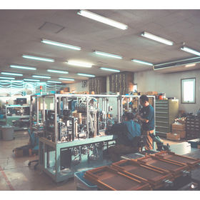
【Fully automated inspection of scratches, dirt, and dimensional defects on ultra-small components】 This is an optimal inspection solution for fields requiring precision processes, such as electronic components, medical devices, and optical devices. Robot transport and AI image analysis work together to highly automate inspections that depend on operators. It has been implemented in research institutions and production lines, achieving high-precision dimensional verification and stable quality assurance. ■ 3D Measuring Instruments Analyzes accurate positions and dimensions even for complex shapes. ■ Surface Roughness Measuring Instruments Quantifies fine surface anomalies and visualizes processing quality. ■ Optical Inspection Equipment Rapidly extracts minute defects, burrs, and scratches through AI image processing. ■ Laser Measuring Instruments Provides stable measurements without contact and is compatible with high-speed lines.

  • DSC00410~2.jpg
  • 設計 (3).jpg
  • 設計 (2).jpg
  • 加工 (6).jpg
  • 加工 (5).jpg
  • 組立1.jpg
  • 川原 (2).jpg
  • 組立4.jpg
  • 電気.jpg
  • Visual Inspection Equipment
  • Other inspection equipment and devices
  • Other analytical and testing equipment
  • Precision machining inspection system

ブックマークに追加いたしました

ブックマーク一覧

ブックマークを削除いたしました

ブックマーク一覧

これ以上ブックマークできません

会員登録すると、ブックマークできる件数が増えて、ラベルをつけて整理することもできます

無料会員登録

Precision Inspection System for Electronic Components

Never miss defects in fine patterns. A high-precision AI automatic inspection solution that supports semiconductor quality.

【AI detects tiny scratches, pattern defects, and dirt with high accuracy】 This is a precision inspection device that meets the strict quality standards required for semiconductor wafers, microchips, and electronic components. By combining advanced image analysis with robotic transport, it significantly automates inspections that rely on visual checks. From ensuring dimensional accuracy to defect detection, it contributes to the stable operation of mass production lines. ■ 3D Measuring Instrument Accurately captures the dimensions of fine structures. ■ Surface Roughness Measuring Instrument Numerically evaluates the finish of electrode and wiring surfaces. ■ Optical Inspection Device Rapidly analyzes tiny defects and pattern abnormalities. ■ Laser Measuring Instrument Non-contact measurement suitable for sensitive electronic components.

  • DSC00410~2.jpg
  • 設計 (3).jpg
  • 設計 (2).jpg
  • 加工 (6).jpg
  • 加工 (5).jpg
  • 組立1.jpg
  • 川原 (2).jpg
  • 組立4.jpg
  • 電気.jpg
  • Visual Inspection Equipment
  • Other inspection equipment and devices
  • Other analytical and testing equipment
  • Precision machining inspection system

ブックマークに追加いたしました

ブックマーク一覧

ブックマークを削除いたしました

ブックマーク一覧

これ以上ブックマークできません

会員登録すると、ブックマークできる件数が増えて、ラベルをつけて整理することもできます

無料会員登録